
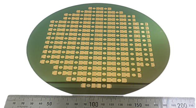
8-Inch-Compatible Wafer Platform
Large-area single-crystal materials are positioned for coupling with 8-inch semiconductor processing to enable scalable MEMS / PIC manufacturing.
iBULe advances piezoelectric MEMS scanners, silicon-compatible processing, smart optics, LiDAR, and photonic actuation technologies through integrated material and device R&D.
The R&D roadmap connects large-diameter crystal growth with 8-inch-compatible processing, MEMS mirror actuation, smart optics, LiDAR, and photonic integration.
Large-area single-crystal materials are positioned for coupling with 8-inch semiconductor processing to enable scalable MEMS / PIC manufacturing.
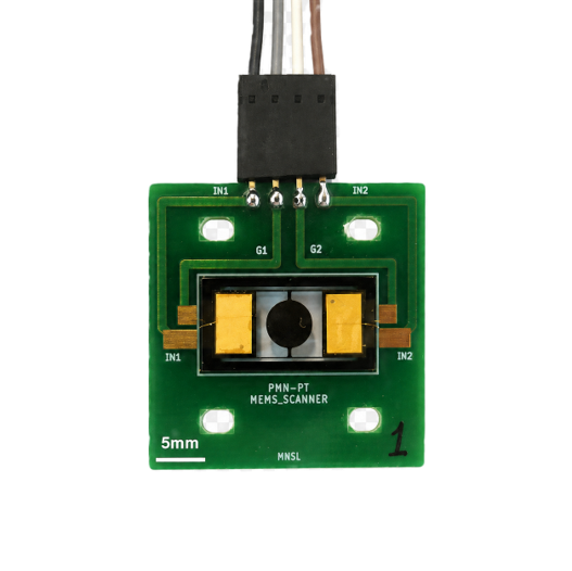
The MEMS scanning mirror architecture is designed for low-voltage drive, simplified assembly, and scalable production.
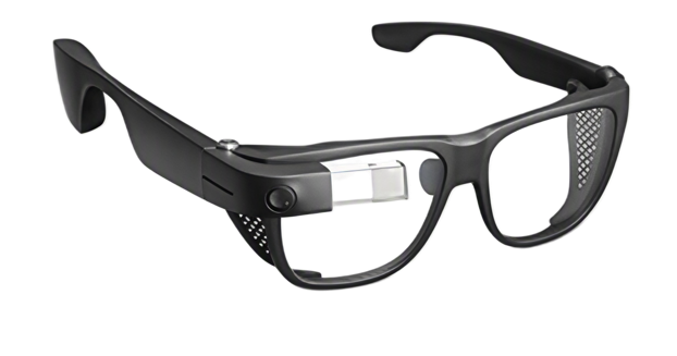
The technology direction extends toward AR/VR smart-glass optical systems where compact, low-power beam steering is critical.
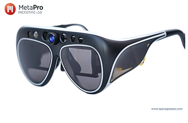
MEMS scanning platforms support compact wearable-display and beam-steering architectures for next-generation optical products.
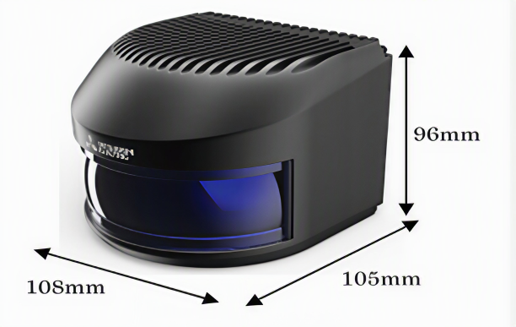
MEMS mirror technology also supports optical scanning for LiDAR-class systems, where size, scan angle, and low-voltage actuation matter.
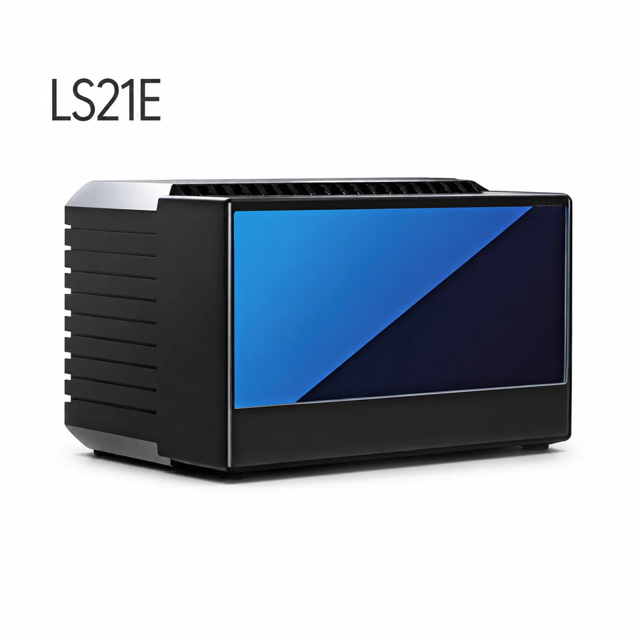
Compact optical-engine form factors extend the platform toward future sensing, wearable, and imaging systems.
A bonded PMN-PT layer applied to a TriPleX® waveguide stack converts voltage into mechanical strain and optical phase control while keeping the actuator outside the optical mode.
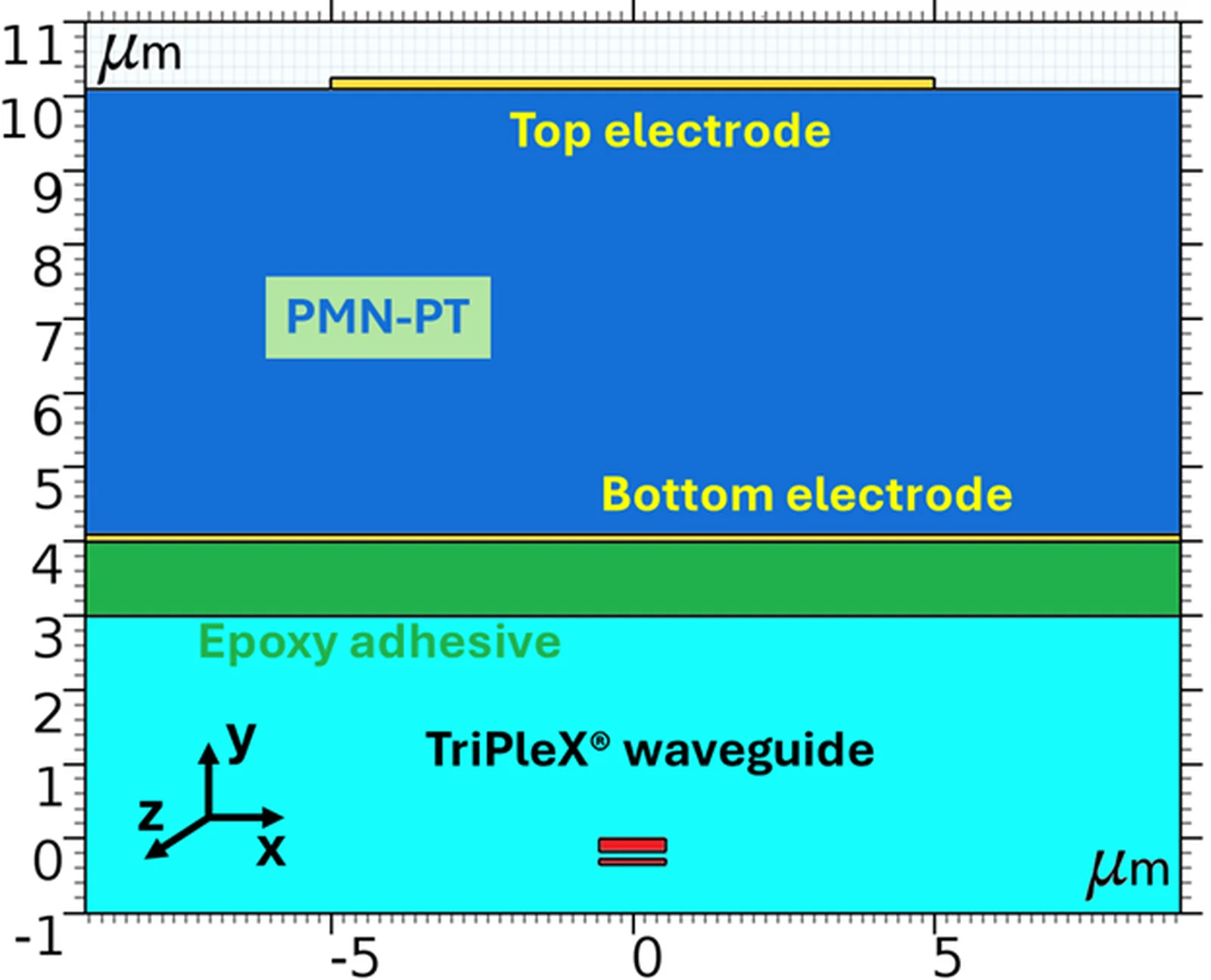
A thin PMN-PT actuator layer, electrodes, and bonded waveguide stack enable photonic modulation and actuation concepts.
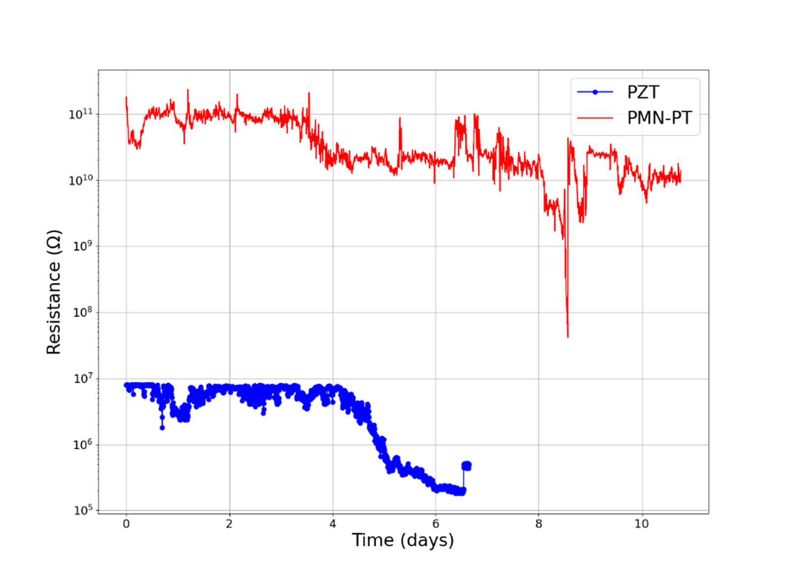
Long-term electrical behavior demonstrates the high internal resistance and low quasi-DC power profile of PMN-PT for photonic actuation.